- 您现在的位置:买卖IC网 > Sheet目录364 > SST25VF020B-80-4C-QAE-T (Microchip Technology)IC FLASH SER 2MB 80MHZ SPI 8WSON
2 Mbit SPI Serial Flash
A Microchip Technology Company
SST25VF020B
Data Sheet
CE#
SCK
MODE 3
MODE 0
0 1 2 3 4 5 6 7
MODE 3
MODE 0
0 1 2 3 4 5 6 7 8 9 10 11 12 13 14 15 16 17 18 19 20 21 22 23
STATUS
STATUS
REGISTER
REGISTER 1
SI
50 or 06
01
7 6 5 4 3 2 1 0 7 6 5 4 3 2 1 0
SO
MSB
MSB
HIGH IMPEDANCE
MSB
MSB
1417 EWSR1.0
Figure 21: Enable-Write-Status-Register (EWSR) or Write-Enable (WREN) and
Write-Status-Register (WRSR) Word-Data Input Sequence
The WRSR instruction can either execute a byte-data or a word-data input. Extra data/clock input, or
within byte-/word-data input, will not be executed. The reason for the byte support is for backward com-
patibility to products where WRSR instruction sequence is followed by only a byte-data.
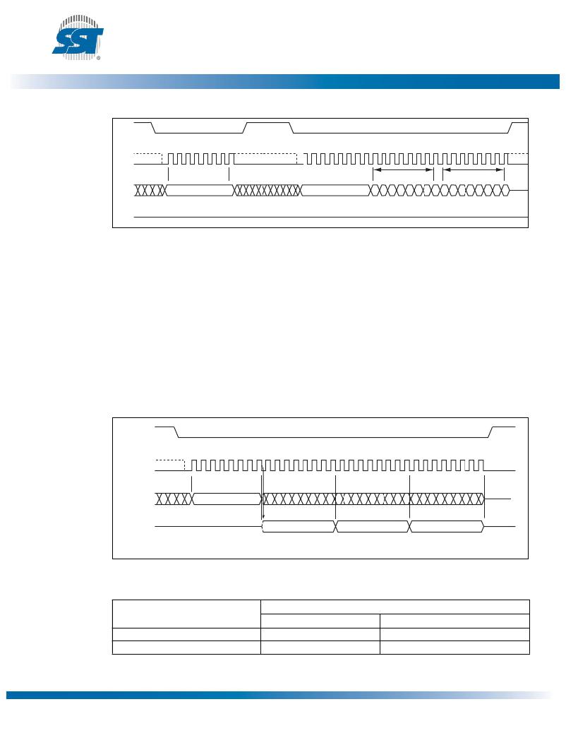
JEDEC Read-ID
The JEDEC Read-ID instruction identifies the device as SST25VF020B and the manufacturer as SST.
The device information can be read from executing the 8-bit command, 9FH. Following the JEDEC
Read-ID instruction, the 8-bit manufacturer’s ID, BFH, is output from the device. After that, a 16-bit
device ID is shifted out on the SO pin. Byte 1, BFH, identifies the manufacturer as SST. Byte 2, 25H,
identifies the memory type as SPI Serial Flash. Byte 3, 8CH, identifies the device as SST25VF020B.
The instruction sequence is shown in Figure 22. The JEDEC Read ID instruction is terminated by a low
to high transition on CE# at any time during data output.
CE#
MODE 3
0 1 2 3 4 5 6 7 8 9 10 11 12 13 14 15 16 17 18 19 20 21 22 23 24 25 26 27 28 29 30 31
SCK
SI
MODE 0
9F
SO
HIGH IMPEDANCE
BF
25
8C
MSB
MSB
1417 JEDECID.1
Figure 22: JEDEC Read-ID Sequence
Table 7: JEDEC Read-ID Data
Device ID
Manufacturer’s ID
Byte1
BFH
Memory Type
Byte 2
25H
Memory Capacity
Byte 3
8CH
T7.0 25054
?2012 Silicon Storage Technology, Inc.
23
DS25054A
01/12
发布紧急采购,3分钟左右您将得到回复。
相关PDF资料
SST25VF032B-66-4I-S2AF
IC FLASH SER 32M 66MHZ SPI 8SOIC
SST25VF040B-50-4C-ZAE
IC FLASH SER 4MB 80MHZ SPI 8CSP
SST25VF040B-80-4I-QAE
IC FLASH SER 4MB 80MHZ SPI 8WSON
SST25VF064C-80-4I-Q2AE-T
IC FLASH SER 64M DUAL I/O 8WSON
SST25VF080B-80-4I-QAE-T
IC FLASH SER 8MB 50MHZ SPI 8WSON
SST25VF512-20-4C-SAE-T
IC FLASH SER 512K 20MHZ 8SOIC
SST25VF512A-33-4I-QAE-T
IC FLASH SER 512KB 33MHZ 8WSON
SST25WF040-40-5I-QAE-T
IC FLASH SER 4MB 40MHZ SPI 8WSON
相关代理商/技术参数
SST25VF020B-80-4C-SAE
功能描述:闪存 2M (256Kx8) 80MHz 2.7-3.6V Commercial RoHS:否 制造商:ON Semiconductor 数据总线宽度:1 bit 存储类型:Flash 存储容量:2 MB 结构:256 K x 8 定时类型: 接口类型:SPI 访问时间: 电源电压-最大:3.6 V 电源电压-最小:2.3 V 最大工作电流:15 mA 工作温度:- 40 C to + 85 C 安装风格:SMD/SMT 封装 / 箱体: 封装:Reel
SST25VF020B-80-4C-SAE-T
功能描述:闪存 2.7V to 3.6V 2Mbit SPI Serial 闪存 RoHS:否 制造商:ON Semiconductor 数据总线宽度:1 bit 存储类型:Flash 存储容量:2 MB 结构:256 K x 8 定时类型: 接口类型:SPI 访问时间: 电源电压-最大:3.6 V 电源电压-最小:2.3 V 最大工作电流:15 mA 工作温度:- 40 C to + 85 C 安装风格:SMD/SMT 封装 / 箱体: 封装:Reel
SST25VF020B-80-4I-Q3AE
功能描述:闪存 2.7V to 3.6V 2Mbit SPI Serial 闪存 RoHS:否 制造商:ON Semiconductor 数据总线宽度:1 bit 存储类型:Flash 存储容量:2 MB 结构:256 K x 8 定时类型: 接口类型:SPI 访问时间: 电源电压-最大:3.6 V 电源电压-最小:2.3 V 最大工作电流:15 mA 工作温度:- 40 C to + 85 C 安装风格:SMD/SMT 封装 / 箱体: 封装:Reel
SST25VF020B-80-4I-Q3AE-T
功能描述:闪存 2.7V to 3.6V 2Mbit SPI Serial 闪存 RoHS:否 制造商:ON Semiconductor 数据总线宽度:1 bit 存储类型:Flash 存储容量:2 MB 结构:256 K x 8 定时类型: 接口类型:SPI 访问时间: 电源电压-最大:3.6 V 电源电压-最小:2.3 V 最大工作电流:15 mA 工作温度:- 40 C to + 85 C 安装风格:SMD/SMT 封装 / 箱体: 封装:Reel
SST25VF020B-80-4I-QAE
功能描述:闪存 2M (256Kx8) 80MHz 2.7-3.6V Industrial RoHS:否 制造商:ON Semiconductor 数据总线宽度:1 bit 存储类型:Flash 存储容量:2 MB 结构:256 K x 8 定时类型: 接口类型:SPI 访问时间: 电源电压-最大:3.6 V 电源电压-最小:2.3 V 最大工作电流:15 mA 工作温度:- 40 C to + 85 C 安装风格:SMD/SMT 封装 / 箱体: 封装:Reel
SST25VF020B-80-4I-QAE-T
功能描述:闪存 2.7V to 3.6V 2Mbit SPI Serial 闪存 RoHS:否 制造商:ON Semiconductor 数据总线宽度:1 bit 存储类型:Flash 存储容量:2 MB 结构:256 K x 8 定时类型: 接口类型:SPI 访问时间: 电源电压-最大:3.6 V 电源电压-最小:2.3 V 最大工作电流:15 mA 工作温度:- 40 C to + 85 C 安装风格:SMD/SMT 封装 / 箱体: 封装:Reel
SST25VF020B-80-4I-SAE
功能描述:闪存 2M (256Kx8) 80MHz 2.7-3.6V Industrial RoHS:否 制造商:ON Semiconductor 数据总线宽度:1 bit 存储类型:Flash 存储容量:2 MB 结构:256 K x 8 定时类型: 接口类型:SPI 访问时间: 电源电压-最大:3.6 V 电源电压-最小:2.3 V 最大工作电流:15 mA 工作温度:- 40 C to + 85 C 安装风格:SMD/SMT 封装 / 箱体: 封装:Reel
SST25VF020B-80-4I-SAE
制造商:Microchip Technology Inc 功能描述:MEMORY FLASH 2M SPI 8SOIC
